EE Times: Novel dry deposition revolutionizes carbon nanotubes
By Juha Kokkonen, published in EE Times on June 21st, 2024.
In today’s semiconductor manufacturing industry, the most advanced chips are produced at 7 nm and below where there is little room for error. Despite the difficulty and unrelenting pressures found in this microworld, engineers and scientists remain undeterred in their pursuit of cutting-edge processes, techniques or materials that push the boundaries of Moore’s Law. Through endless experimentation at the nanoscale level, designers and researchers seek to uncover minute improvements that have the potential to translate into millions—if not billions—of dollars in revenue for chipmakers.
The emergence of carbon nanotubes (CNTs) as a compelling alternative material to address inefficiencies in extreme ultraviolet (EUV) lithography has the potential to be one of those innovations. However, contemporary production methods create CNTs that fall short of expectations. To realize the full potential of CNTs requires a new production method that significantly improves their quality. Only then can they help the semiconductor industry deliver on the insatiable demands for advanced chips.
EUV lithography and chipmaking
Before exploring the production methods behind creating CNTs, one must first understand why they are so crucial in the semiconductor industry.
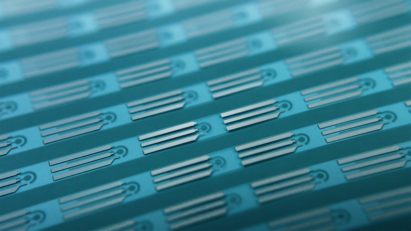
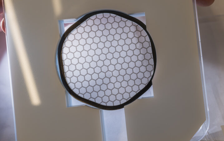
It starts with EUV lithography, which is the process in chipmaking where EUV light prints the chip’s pattern on a silicon wafer from a template that houses the chip’s circuitry pattern, known as a photomask. Before use, the masks are inspected for defects in an EUV mask inspection machine, with debris filters keeping the optics of the mask inspection tool clean, ensuring error-free inspection. After the mask is made and placed into the EUV scanner, a pellicle—an ultra-thin membrane—is mounted on the mask to prevent particles from landing on the mask. And, as it turns out, membranes composed of different materials will perform this important task differently. The experimentation with different materials to improve their protective capabilities is where CNT membranes come in.
Yet, even in the most controlled environments, errors can happen when producing sub-7-nm chips. During the EUV process, if dust particles end up on the photomask during imprinting, the pattern imprinted on the wafer will be defective and lead to costly and expensive chip failure. To protect the photomask from particles that can contaminate its pattern when imprinting, chipmakers affix thin membranes onto the photomask to filter out the presence of nanoparticle contaminants and prevent defects. These thin membranes, known as EUV pellicles, not only possess crucial protective properties but also enable the high transmittance of EUV light required for imprinting.
It is this outsized role played by EUV pellicles in preventing costly chip failure—the concern of every chipmaker, fab and foundry—that makes the underlying material used in their composition a matter of great consequence.
The nanocarbon revolution
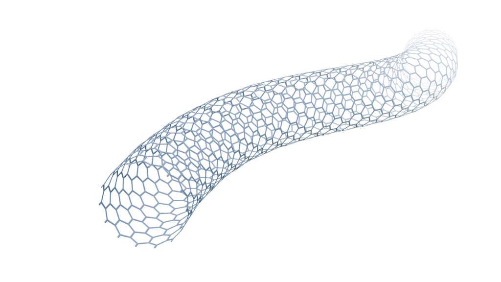
Since their discovery in the 1990s, CNTs emerged from the lab to become a compelling advanced material for many applications. But it is their potential application as a nanomaterial in semiconductor manufacturing that has not been well understood or executed. Based on carbon—the most versatile material in the universe—a CNT is a graphene rolled into a cylinder that exhibits tremendous physical properties for enhancing electrical, mechanical, optical, chemical and thermal properties.
After chipmakers migrated from optical to EUV lithography, the role of pellicles in chipmaking was altered significantly. During the new EUV process, chipmakers faced challenges when protecting the photomask. In response, chipmakers created an accompanying EUV-specific pellicle to address them. It was not until the underperformance of EUV pellicles made of polysilicon that the industry began experimenting with new alternative materials, such as CNTs, as a better replacement material.
Improving the method
While EUV pellicles composed of this promising new nanomaterial are an improvement over previous materials, the industry needs to reexamine how it produces CNTs if it wants to realize their full potential. Traditional CNT manufacturing processes often use harsh techniques like liquid dispersion and ultrasonication, which can damage the delicate structures of CNTs, hindering their full potential of exceptional transmittance, uniformity and robustness. In fact, this incumbent production methodology, known as wet dispersion, compromises CNT strength and performance through outright bundling, contamination and shorter lengths of the individual CNTs. Dispersing CNTs into the liquid cuts damages them, resulting in significantly lower transmittance and reduced tensile strength. Chipmakers utilizing EUV pellicles composed of these lower-quality CNTs run the risk of underperforming in the intensity and heat of EUV lithography.
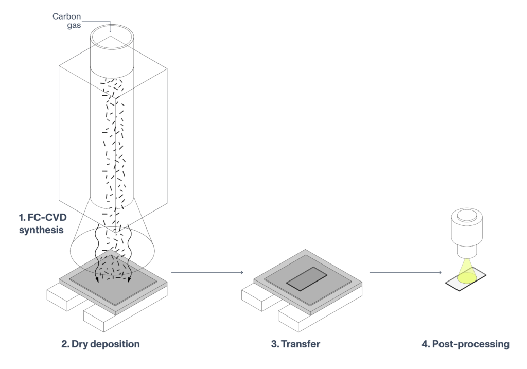
In response, nanomaterials experts created alternative production methods that preserve and do not hinder the properties of CNTs. A methodology that has overcome these challenges is Dry Deposition, a method invented and patented by Canatu. Novel dry deposition bypasses the traditional wet dispersion of CNTs—which threatens or compromises the overall integrity of CNTs—to produce superior long and pristine CNTs.
Dry deposition technology surpasses the more harsh and excessively complex need for costly multi-step production. The result is longer, cleaner, and nearly defect-free CNTs with superior uniformity, transmittance, and tensile strength of the individual tubes (over 10× stronger than steel) thanks to their increased length and purity. Most importantly, these CNTs preserve high EUV light transmittance, making them the perfect candidate for enhancing performance in EUV lithography.
Chip success
Back in the fab, the downstream impact of dry deposition manufacturing is clear. Using EUV pellicles composed of CNTs produced via dry deposition in EUV lithography will better protect the photomask from defects, while enhancing precision and shortening processing. Put simply, the decrease of contaminated particles on the photomask reduces the number of defects and with it the (costly) rate of chip failure. The results are a 15% increase in productivity (measured in wafers per hour) compared to the traditional EUV pellicles in use for semiconductor applications (and additional cost savings due to a reduced need for expensive ASML lithography machines). Further, their increased toughness puts them in the lead as the most promising material for EUV pellicles used in the next-gen, high-power scanners.
To deliver on the short- to mid-term demand for AI and next-gen chips of the future, we anticipate chipmakers will continue to seek out gains in productive output and cost reduction wherever possible. At the same time, they will build the groundwork for the technology and advanced materials that support the more powerful chips of the future.
—Juha Kokkonen is CEO of Canatu.
Contact the author