Industry coverage: How carbon nanotubes can transform the semiconductor industry
By Juha Kokkonen, published in Electronic Design on Jan.10, 2025.
Carbon nanotubes present a game-changing solution for preventing defects in EUV lithography, supporting the semiconductor industry’s drive toward extreme miniaturization and improved chip reliability.
What you’ll learn:
- The critical role of EUV pellicles: These thin membranes protect photomasks from contaminants, reducing defect rates and ensuring flawless chip production.
- The limitations of traditional materials: Current EUV pellicles struggle to withstand the extreme conditions of high-power EUV scanners, leading to performance issues.
- The potential of carbon nanotubes: CNT-based EUV pellicles offer exceptional properties like high transmittance, low flare, and high heat resistance, making them a promising solution for the future of chipmaking.
Fueled by the proliferation of artificial intelligence and hyperconnectivity, the semiconductor industry is predicted to double in size within the next decade. Yet while microchips, the tiny powerhouses that underpin everything from our smartphones to lifesaving medical devices, are experiencing historic demand, they also face a looming technical impasse.
Miniaturization Challenges in High-NA EUV Lithography
The relentless miniaturization of transistors, down to 3 nm and below, demands flawless execution and fabrication. Throughout the 2000s, this incredible shrinking trend (from 90 nm to 7 nm and smaller) ushered in a new era of technological advancement.
In the last decade, we witnessed the astonishing feat of fitting 50 billion transistors onto a single chip. This achievement was possible due to extreme ultraviolet (EUV) lithography, a cutting-edge process that uses EUV light. EUV lithography can print much finer integrated-circuit (IC) patterns than previously possible because its wavelength (13.5 nm) is much shorter than that traditionally used in conventional deep ultraviolet (DUV) lithography (193 nm).
Leaders in semiconductor manufacturing are rushing to deploy these systems in high-volume production, with the first High Numerical Aperture (High-NA) EUV tools already installed. These complex machines promise to reduce feature size further while boosting production efficiency. However, despite the advances, the critical challenge of achieving zero defects during the EUV lithography process remains.
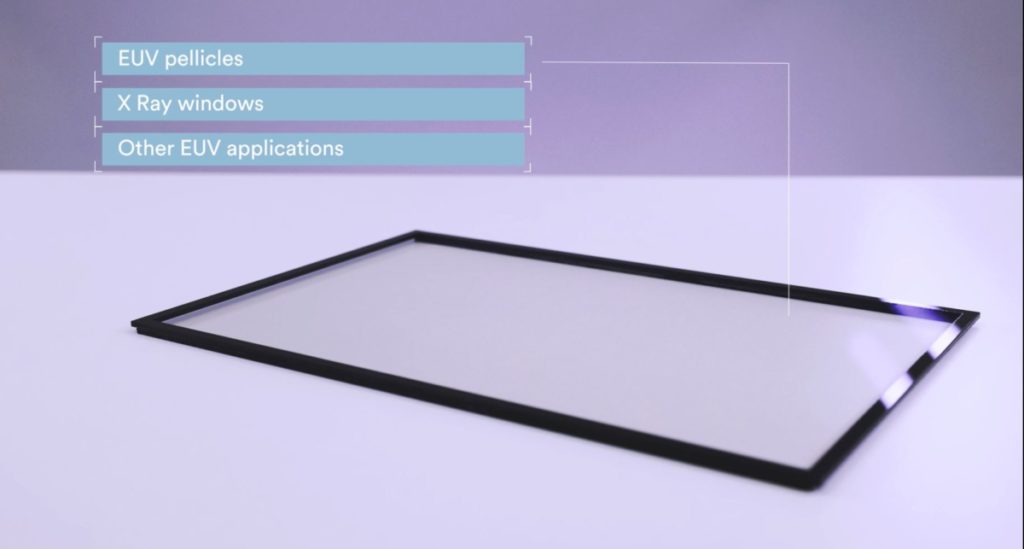
Manufacturers recognize that EUV pellicles (Fig. 1)—a thin, transparent membrane placed over the photomask to protect it from contaminants—are critical for overcoming this hurdle. By intercepting particles before they land on the EUV mask containing the blueprint for the chips, EUV pellicles can significantly reduce defect rates, bringing the industry closer to the goal of zero defects.

The Defect Dilemma in EUV Chip Manufacturing
Defects continue to negatively impact the performance and reliability of the chips produced today. It’s important to minimize errors throughout every step of the chip manufacturing process. An EUV mask is a highly precise template used in the semiconductor manufacturing process to create intricate patterns on silicon wafers. It acts as a stencil, blocking certain areas of the wafer from exposure to EUV light, which etches the desired patterns onto the silicon.
In the initial phase, before the EUV mask even enters the scanner, three common types of defects may occur: Surface imperfections, which make up many observed defects, are caused by underlying material being exposed during the layering process. Next, tiny particles trapped within the layers can come from the initial material or from handling during construction. Finally, the layering process may unintentionally create defects on the surface of the mask, either fully or partially covered.
Defects could also be introduced to the photomask in the next stage, as the EUV scanner itself may be a source of imperfections. The extreme conditions within the scanner, such as high temperature and high power levels, can introduce defects onto the mask during exposure.
As temperatures rise close to 1,000°C during high-power EUV lithography, conventional EUV pellicles offer protection, but their deterioration during processing can compromise both the mask and scanner through mechanisms like heat warping or contaminant release. On top of that, if pellicles made from conventional metal silicide break, they shatter like glass, causing unwanted, costly downtime.
Carbon-nanotube (CNT) membranes excel at filtering contaminants to safeguard the photomask, but their capabilities extend beyond this primary function and have been well understood at Canatu. Though the ultra-thin CNT network designed for EUV pellicles can maximize EUV transmittance while maintaining excellent particle filtration, thicker and more robust Canatu CNT membranes could also be used as debris filters for actinic mask inspection. This special technique is used to inspect photomasks before the EUV mask enters the scanner.
Even with all of today’s advances in semiconductor manufacturing, preventing defects caused by harmful particles on the photomask remains a manufacturing challenge. Ideally, by controlling and reducing the presence of impurities, fabs can enhance yield, leading to more consistent chip performance. Yet performance in this realm has remained stubbornly stilted.
The Role of Carbon Nanotubes in EUV Lithography Efficiency
The potential of CNTs for use in EUV pellicles to protect the photomask from defects during EUV lithography has only come into sharper focus in recent years. In fact, CNT pellicles are a key enabler of higher yields and performance in EUV lithography: CNT pellicles are estimated to increase productivity by 7% to 15% due to their higher transmittance, enabling the next step in semiconductor performance.
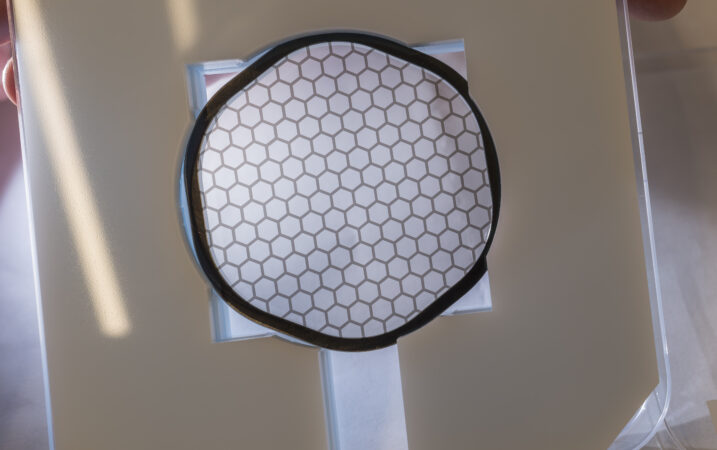
Canatu develops advanced CNT membranes (Fig. 2) for EUV pellicles, offering a unique combination of properties. Uncoated Canatu CNT membranes feature high transmittance at EUV (> 97%T), minimal flare (< 0.2%) and high thermal stability in a vacuum (> 1,500°C).

High transmittance translates to more EUV light passing through the pellicle to reach the wafer, increasing throughput. Low flare (scattering) ensures even the tiniest features can be printed on the wafer with high precision without pattern distortion. High heat resistance, chemical inertness, and high tolerance to pressure differentials ensure CNT membrane-based EUV pellicles can withstand the next-gen high-power scanner environment’s intense vacuuming and venting cycles while sustaining their optical properties.
According to ASML, the most cutting-edge High-NA EUV scanners will introduce high power levels exceeding 500 W, increasing the optical system’s ability to focus and collect light (i.e., numerical aperture [NA] from 0.33 to 0.55), providing higher-resolution imaging capabilities. The increase in power levels directly contributes to more wafers per hour (WPH). For instance, a 400-W source enables a throughput of 160 wafers per hour, while 500 W can print more than 185 wafers per hour.
However, the higher power levels and mask (reticle) stress will generate high heat loads that traditional materials can’t withstand, causing pellicle deformation or, in other cases, causing the pellicle to shatter like glass.
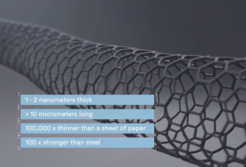
To echo ASML’s recent comments during the 2023 SPIE Conference, carbon nanotubes (Fig. 3) are emerging as the most promising material for EUV pellicles for high-power scanners. Continued research and development in CNT membrane-based EUV pellicle technology is crucial to unlocking its full potential, but the promise it holds for the future of chipmaking is undeniable.

CNT Pellicles: Purity for Precision Chips
As EUV lithography revolutionizes the semiconductor manufacturing industry, CNT membranes are the ideal choice for protecting the photomask from contamination during the mask inspection and EUV lithography process while ensuring cleaner and more precise chip production. The exceptional properties of CNTs make them a versatile and future-proof material for EUV lithography, promising fewer defects, supporting higher yield rates, and ultimately enabling the production of smaller, faster and more reliable chips—the cornerstone of our ever-evolving technological landscape.
Contact the author


