Semiconductor Digest: Roadblocks to significant yield and cost improvement for chip manufacturers
By Juha Kokkonen, published in Semiconductor Digest‘s Aug/Sep issue 2024.
In chipmaking, a single defect can ruin an entire silicon wafer worth $20,000, a costly margin of error that can accumulate into millions and even billions of losses in the production ledger over time. Chipmakers painstakingly work to reduce defects, yet the introduction of any innovation to protect against them and prevent costly chip failure must be balanced against maintaining the harmony of a near endless set of components, tools, and intricacies all carefully calibrated to engineer maximum output. Therefore, increasing the protection of these expensive parts must not come at the expense of slower production, or else chipmakers will face financial losses like those they sought to ameliorate
Yet in 2024, semiconductor manufacturers face a perfect storm of factors that has turned the delicate and difficult balancing act of yield and cost improvement into a high-stakes tight-rope walk. Chipmakers must achieve a reduction in defects on the smallest chips to date, in the most expensive machines, for the most demanding production environments ever seen, all amidst historic demand. While next gen ASML machines are ready for delivery to chipmakers who are racing to deliver chips with ever-smaller, record-breaking node sizes, the challenges presented by defects have not been resolved. Critical enablers that can thread this complex set of factors and restore maximum output and profitability will take on a major significance in the coming years.
The AI chips arms race
Smaller nodes, which provide improved performance, increased power efficiency, and higher transistor density, are the key to powering Big Tech’s cloud, artificial intelligence (AI), and machine learning (ML) next-generation applications that require high computation power in a small package. With the arrival of generative AI, the future of tech now depends on the ability for tech companies to quickly ascertain the necessary underlying chips to power their new AI services. Endearingly nicknamed the “AI chips arms race”, the rush to provide Big Tech with the most powerful chips on a large scale has, in turn, put enormous pressure on chipmakers to find manufacturing productivity gains, what is known in technical terms as throughput.
The major chip companies are jockeying for top position by announcing new next-gen capabilities and ever-smaller node sizes to woo tech companies to choose them for the chips needed for their AI products. Meanwhile, if secured, the capacity additions needed to scale up production for that kind of fulfillment are staggering. According to the latest projections from Deloitte, 2024 is now predicted to see global chip sales of $588 billion, a 13% increase compared to 2023, and 2.5% higher than 2022’s record industry revenues of $574 billion.
Any methodology, tool, or technology that can help semiconductor manufacturers create the most innovative and powerful chips with the smallest node sizes on a large enough scale to meet demand will take on outsized importance to chipmakers.
Why EUV?
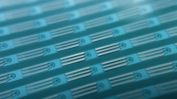
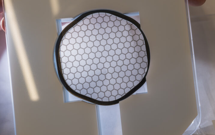
Extreme Ultraviolet (EUV) lithography is used in chipmaking to print a chip’s pattern on a wafer from a photomask, which is the template that houses the chip’s circuitry pattern, using EUV light. If dust particles end up on the photomask during imprinting, the pattern imprinted on the wafer will be defective, causing costly chip failure and poor yield. To protect the photomask from particles that can contaminate its pattern when imprinting, chipmakers affix thin membranes onto the photomask to filter out the presence of nanoparticle contaminants that can cause defects. These thin membranes, known as EUV pellicles, possess crucial protective properties while enabling the high EUV light transmission required for imprinting. Most importantly, advancements in extreme ultraviolet lithography machines gave chipmakers the chip-making density to achieve ever-smaller, record-breaking node sizes in full accordance with Moore’s Law.
The temperature rises
In 2013 ASML’s first gen EUV lithography systems provided chipmakers with smaller wavelengths of light for imprinting, which gave them the ability to print the tiniest features. The precision of its new groundbreaking High NA machine will be within reach of manufacturers for approximately $400 million while the first gen EUV lithography machine is priced at $150 million. Today, chipmakers have achieved 3nm node size and are locked in battle to win the race to 2nm (node sizes serve as an informal placeholder measurement of innovation where the node size indicates the smallest feature possible on a transistor, providing a metric of overall transistor size).
But with this new machine comes a new production environment with a new set of performance demands and requirements for operation. The next-gen, pricey high-NA ASML scanner will introduce high power levels exceeding 500W. These higher power levels put higher heat loads and mechanical stress on all components, including EUV pellicles. These components must not only survive in these new harsher conditions but perform flawlessly.
On top of the need for components that can perform at the highest possible level in the hottest and most extreme environments to date, the operation of these expensive ASML machines brings with them major financial considerations. Semiconductor manufacturers must fully maximize production on a single EUV machine to avoid the need to acquire an additional several hundred-million-dollar EUV machine to meet their capacity goals. Yet, fully operationalizing the machine’s capabilities to squeeze out every possible unit in terms of efficiency cannot risk damaging the machine or even contribute to its wear and tear and maintenance needs. Additional unscheduled maintenance will pull the machine out of service, dropping output to zero for an unspecified amount of time.
The carbon nanotube solution
It falls to chipmakers to assemble and fine-tune the ingredients and recipe for success amid all these variables and constraints. But among the exhaustive search for new advanced materials that could flourish in the specific conditions of this era of chipmaking, carbon nanotubes (CNTs) are at the top of the list.
First emerging from the laboratory in the 1990’s, CNTs became the most promising alternative material for EUV components like EUV pellicles and debris filters due to their unique combination of properties: high EUV transmission, mechanical strength, and high heat resistance. High EUV transmission, combined with the exceptional mechanical and thermal properties of CNTs, addresses the middling performance of a previous generation’s membranes. Silicon-based pellicles require considerably higher thickness due to their weak mechanical properties, which causes detrimental absorbance of the necessary EUV light for imprinting. If the pellicle breaks inside the scanner due to an unexpected failure, traditional silicon pellicles break like glass, causing contamination and significant downtime. CNT-based EUV pellicles avoid this issue due to the fibrous crystal structure, which allows them to fracture like paper, thereby minimizing contamination.
EUV pellicles using CNT membranes offer higher EUV light transmission, heat resistance, chemical inertness, and high-pressure tolerance, ensuring durability in ASML’s next-gen scanners. The result is greater productivity, efficiency, and yield while extending the EUV light source’s lifetime (and thus longer service intervals).
The road to 2026
It is no surprise then that at the SPIE conference held in San Diego in February 2023, ASML stated that CNTs are the most promising material for EUV pellicles for their high-power scanners. To meet future demand, ASML plans to add capacity to less-advanced low-NA EUV (90) and deep lithography DUV machines (600) for 2025-2026, while also ramping up High-NA EUV capacity (to 20 systems) by 2027-2028. Therefore, the heat is on chipmakers to solve the problems that have hamstrung their capabilities (and profits) now that orders have been placed and these machines are effectively on the way. After all, they themselves have signed contracts with tech companies promising advanced, next gen chips by a certain date.
Adding to the progression of CNT development, Canatu has created its own CNTs and CNT membranes for EUV pellicles which surpass the performance capabilities of today’s EUV pellicles. Thanks to Canatu’s novel Dry Deposition™ methodology, CNTs of higher quality with additional performance gains are now on the table. CNT membrane-based EUV pellicles can enable a 7-15% improvement in performance (wafers per hour), a massive increase and substantial edge in output that can translate to “make-or-break” manufacturing returns. As the industry gears up to meet its biggest challenge yet, the potential of CNTs as the missing puzzle piece for a daunting matrix of factors, challenges, and considerations cannot be overlooked.
Contact the author