SEMICON Europa 2023
During the Executive Forum on Materials Innovation at SEMICON Europa 2023 Emma Salmi, Head of Synthesis, presented ‘Canatu carbon nanotube membranes as a versatile material platform for EUV lithography.’ She highlighted the benefits of our unique carbon nanotube manufacturing process, emphasized the expertise gained from mass-producing EUV membranes since 2021, and elaborated on the customization of these membranes for diverse applications, highlighting remarkable versatility they offer.
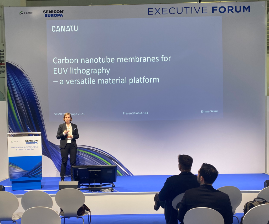
Carbon nanotube membranes for EUV photolithography – a versatile material platform
Attendees gained insights into the benefits of Canatu’s floating catalyst chemical vapor deposition (FC-CVP) process using dry deposition method, which yields long and pristine carbon nanotubes enabling better performance in the end applications. High control over the synthesis allows tailoring of carbon nanotube network density, bundle size, tube diameter, and wall count. The direct fabrication method with tailorable morphology combined with the exceptional mechanical and thermal properties of carbon nanotubes provides a versatile platform technology, which can be further modified with post process steps such as purification to remove metal impurities. Canatu’s carbon nanotube membranes are used e.g. in EUV pellicles.
Emma Salmi is a senior nanomaterials engineer at Canatu. She has been spearheading the development of free-standing carbon nanotube membranes with primary focus on the FCCVD synthesis and early processing steps for optimum pellicle manufacturing for two years. Her background encompasses nanotechnology, thin film deposition systems and carbon nanomaterials with 15 years of industrial and academic experience. She has 37 peer-reviewed publications, conference papers and patents.
Pushing the boundaries for materials and innovations for next-generation technologies
Advanced modern nanoelectronics technology is approaching physical limits and overcoming them has been a core business in technology and manufacturing since in 1965 the late Gordon Moore formulated his seminal findings and predictions, known as “Moore’s Law”. Whenever barriers showed up, that had the potential to slow down the predicted cadence in scaling, innovations came up, which have brought the community to a level, where features of atomic-scale dimensions can be reliably manufactured at many levels with extreme critical (sub-10 nm) dimensions. Materials innovation in particular has always been at the crux of these exciting developments, and even more so with novel device designs using the 3rd dimension as mentioned in recent IDRS roadmaps. And as history also tells us, many materials developed to continue Moore’s Law scaling pace have also found their use for many More than Moore applications. Continuous materials and atomic-scale process innovation are required for applications such as Gate-all-around (GAA) logic, Advanced Memories (VNAND and 3D-DRAM), Advanced Lithography (EUV and high NA-EUV), but also for Beyond Moore applications (graphene and 2D materials), or compound semiconductors used in Power electronics (e.g. gallium nitride in electric grids), Photonics (e.g. Sb- and Bi-based semiconductors in infrared sensors) and Quantum Computing (e.g. InSb semiconductors). Developments and challenges related to atomic-scale processing and control of interfaces, morphology, composition, and 3D conformality for these applications will also be addressed.
Contact