

Semiconductor
Enabling the next step in efficiency
Semiconductors are all around us in every single electronic device we use. That is how they make an impact in our everyday. Progress in the semiconductor industry continues fast driven by Moore’s Law aimed at doubling the transistor density on a wafer every two years. Higher transistor density will lead to more efficient processors and memory chips for the benefit of everyone using electronic devices.
To keep up with the pace of development, the industry has developed extreme ultraviolet lithography (EUV) technology. Using extreme ultraviolet wavelengths, this wafer exposure technology improves resolution and allows producing wafers with transistor node sizes of 7 nm or less.
Canatu CNT plays a key role in advancing the EUV process required for producing the most advanced microchips. Today, Canatu is a prominent supplier of CNT -based products and manufacturing equipment for the semiconductor industry. Our product portfolio includes CNT pellicle membranes, inspection membranes, and optical filters for EUV and X-ray filter applications.
Our products

The world’s thinnest and strongest carbon nanotube membranes, tailorable for your exact needs. Applicable for high-power EUV lithography and X-Ray filter applications. Made of the most advanced carbon nanotubes, known for their exceptional purity and properties.
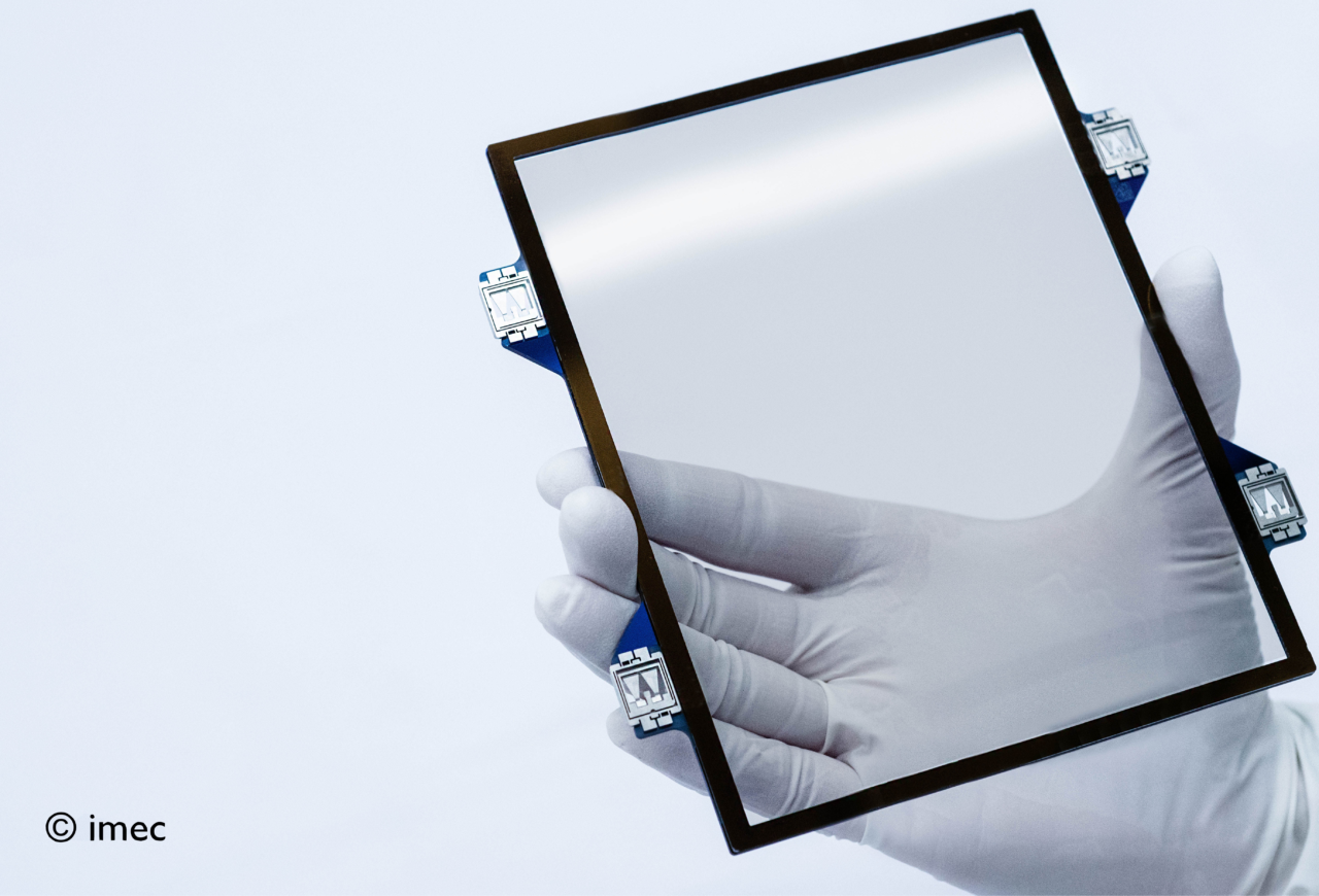
CNT pellicle membranes are used to protect the photomask from contamination while permitting high EUV transmission. Canatu CNT pellicle membranes support the productivity increase potential in the EUV lithography process by up to 8-15%.
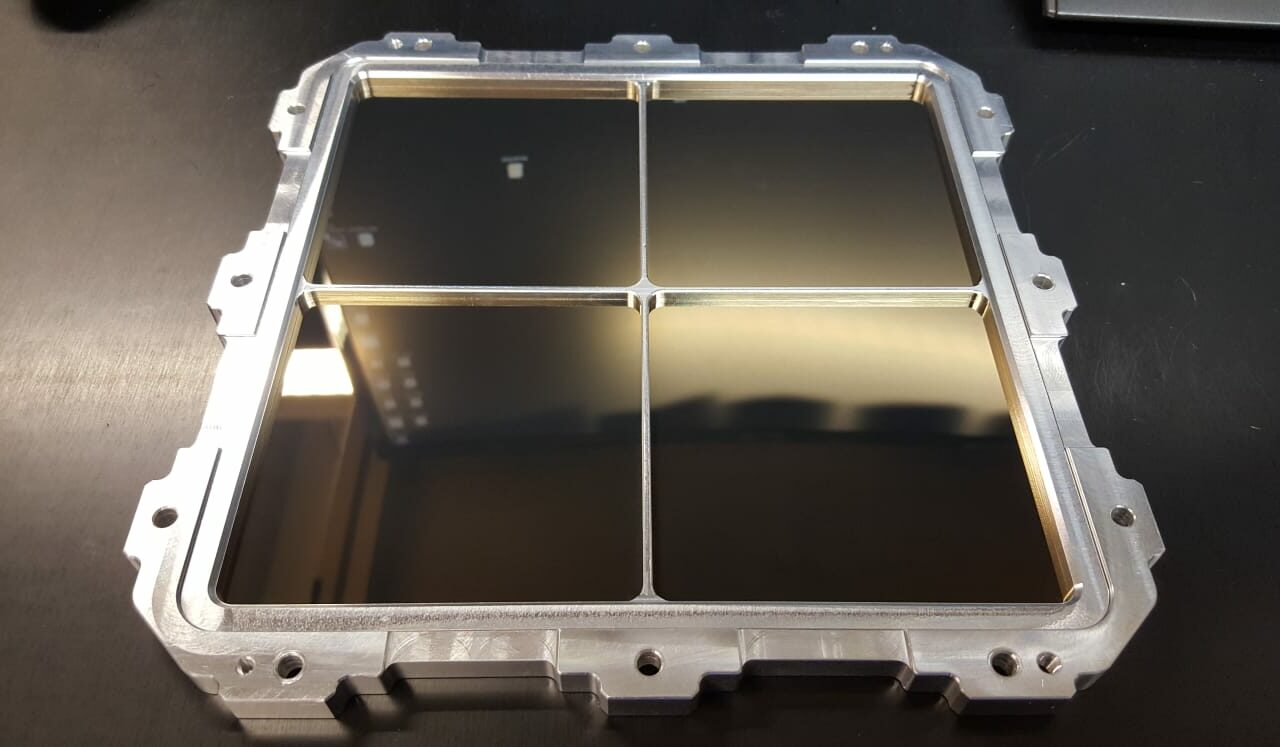
Canatu optical filters block short-wavelength photons and high-energy particles that can interfere with the measurement process, while providing high transmittance for EUV and X-ray wavelengths.
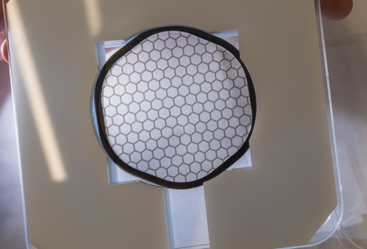
Canatu inspection membranes enhance quality control by filtering debris from the EUV light source and optical path, preventing particle contamination on photomasks. They feature high EUV transmittance for optimal light passage, enabling accurate defect detection.
Taking semiconductors to a smaller scale
As volumes rise in semiconductor manufacturing and ever-smaller features are printed on them, there is greater pressure to avoid defects. Tiny defects lead to errors on the wafer, causing costly yield losses.
Canatu has a unique solution based on CNT membrane to enable nanoscale debris filtering in a demanding environment: high EUV transmittance, low reflection and flare, high heat resistance and mechanical strength.
EUV pellicles are membranes that protect the photomask from particle contamination while permitting EUV transmission. The CNT membrane must be thin enough to limit the imaging impact while robust enough to survive handling.
See video
We partner with forerunner companies ready to transform industries